-
chevron_right
Wearable AI: will it put our smartphones out of fashion?
news.movim.eu / TheGuardian · Sunday, 31 March - 11:00 · 1 minute
Portable AI-powered devices that connect directly to a chatbot without the need for apps or a touchscreen are set to hit the market. Are they the emperor’s new clothes or a gamechanger?
Imagine it: you’re on the bus or walking in the park, when you remember some important task has slipped your mind. You were meant to send an email, catch up on a meeting, or arrange to grab lunch with a friend. Without missing a beat, you simply say aloud what you’ve forgotten and the small device that’s pinned to your chest, or resting on the bridge of your nose, sends the message, summarises the meeting, or pings your buddy a lunch invitation. The work has been taken care of, without you ever having to prod the screen of your smartphone.
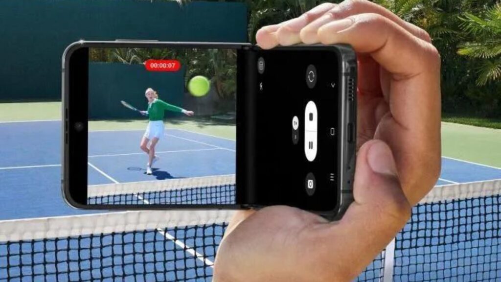
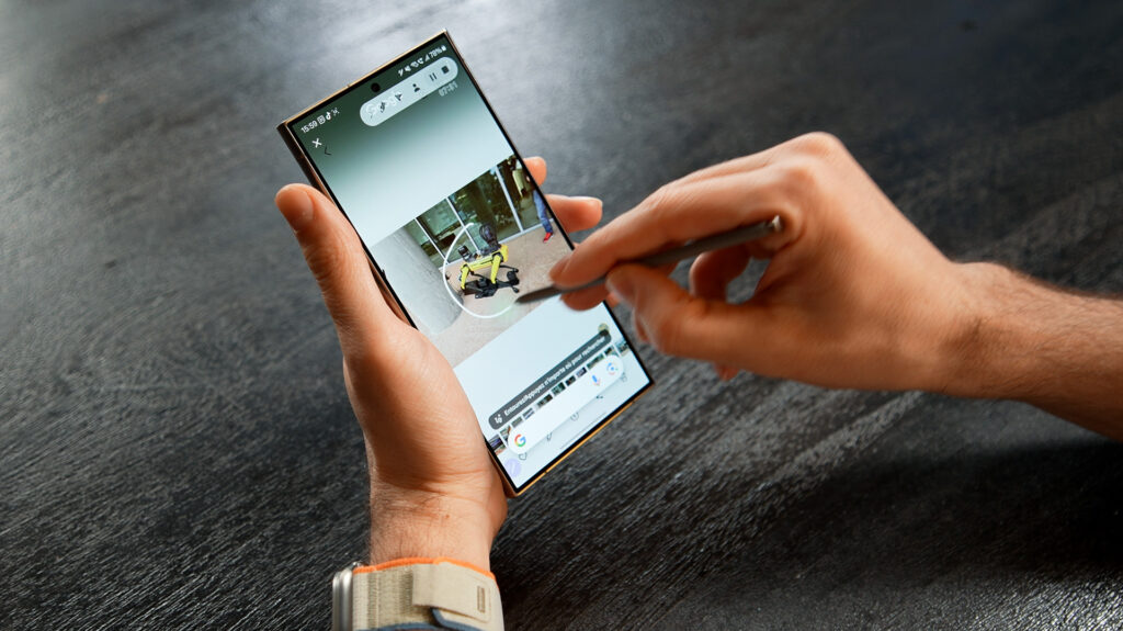
It’s the sort of utopian convenience that a growing wave of tech companies are hoping to realise through artificial intelligence. Generative AI chatbots such as ChatGPT exploded in popularity last year, as search engines like Google, messaging apps such as Slack and social media services like Snapchat raced to integrate the tech into their systems. Yet while AI add-ons have become a familiar sight across apps and software, the same generative tech is now making an attempt to join the realm of hardware, as the first AI-powered consumer devices rear their heads and jostle for space with our smartphones.
Continue reading...


